Amid the heightening competition in the global chip foundry market, Samsung Electronics unveiled a new packaging technology Thursday that would help differentiate its foundry service.
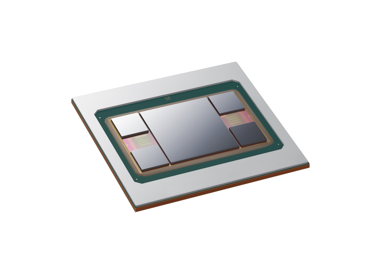
Samsung said it has completed the development of the next-generation 2.5D packaging technology named Interposer-Cube4, or I-Cube4, which is immediately available for customers.
Samsung’s I-Cube is a heterogeneous integration technology that horizontally places one or more logic dies, such as a CPU or GPU, and several high bandwidth memory dies on top of a silicon interposer, meaning that multiple dies operate as a single chip in one package.
In 2018, the company had announced its first I-Cube technology that integrated one logic die with two HBM dies, which was applied to Chinese portal giant Baidu’s artificial intelligence chip Kunlun in 2019.
Samsung’s new I-Cube4, which incorporates four HBMs and one logic die, was designed to help raise the speed of data transmission and power efficiency in the fields of high-performance computing, AI, 5G, cloud and large data center application, according the company.
In general, the silicon interposer area proportionally increases to accommodate more logic dies and HBMs. Since the silicon interposer in the I-Cube is thinner than paper (around 100 micrometers thick), the chances of it bending or warping a larger interposer becomes higher, which negatively impacts product quality.
Samsung studied how to control interposer warpage and thermal expansion by making changes to the material and thickness, and succeeded in commercializing the I-Cube4 solution.
The chipmaker has developed its own mold-free structure for I-Cube4 to efficiently remove heat and enhanced its yield by conducting a pre-screening test that can filter out defective products during the fabrication process.
This method provides additional benefits such as a reduction in the number of process steps, which reduce costs and turnaround time, Samsung said.
Since the launch of I-Cube2 in 2018 and eXtended-Cube (X-Cube) in 2020, Samsung’s heterogeneous integration technology has signaled a new era in the high-performance computing market.
Samsung is currently developing more advanced packaging technologies including I-Cube6 and higher by using a combination of advanced process nodes, high speed interface IPs and advanced 2.5/3D packaging technologies, which will help customers design their products in the most effective way.
“With the explosion of high-performance applications, it is essential to provide a total foundry solution with heterogeneous integration technology to improve the overall performance and power efficiency of chips,” said Kang Moon-soo, senior vice president of foundry market strategy at Samsung. “With the mass-production experience amassed through I-Cube2 and the commercial breakthroughs of I-Cube4, Samsung will wholly support customers’ product implementations.”
By Song Su-hyun (
song@heraldcorp.com)